

Tag: nanotechnology

  • From Nanomaterials to Commercialization: How Dr. Shruti Sharma Identifies Innovation Early

    From Nanomaterials to Commercialization: How Dr. Shruti Sharma Identifies Innovation Early

    Dr. Shruti Sharma, a materials scientist and innovation ecosystem builder, has built a career around recognizing potential long before it becomes obvious to others. Her journey from nanomaterials research to technology commercialization offers a unique perspective on how to evaluate and support early-stage technologies.

    Sharma’s training in materials science taught her to look below the surface. In the lab, she studied how materials behave at the nanoscale—how structures change, particles interact, and properties emerge. That habit of close observation now shapes her work with startups, commercialization programs, and innovation ecosystems.

    After research stints at Brookhaven National Laboratory, Sharma moved into applied research and venture development. She has mentored more than 100 startups across clean energy, life sciences, advanced materials, and AI-enabled technologies. Her focus is on helping deep tech teams navigate the gap between scientific promise and real-world impact.

    Sharma emphasizes that early technologies need more than encouragement—they need rigorous questioning. What has been proven? What assumptions remain untested? What would make a customer or partner take the technology seriously? By asking these questions, she helps founders build credible paths to market.

    Her work at the Long Island High Technology Incubator included designing venture development programs that systematically reviewed emerging technologies. In the first months, more than two dozen technologies and startups were assessed. For Sharma, the value lay in creating a process that forced serious ideas to confront the right questions early.

    She has also contributed to Department of Energy-funded commercialization efforts focused on clean energy innovation and technology transfer. Her role often involves partnership-building, program design, and evaluation metrics—the structural elements that determine whether a breakthrough becomes usable.

    Sharma’s commitment to mentorship extends beyond formal programs. She co-founded Vigyanshaala, a grassroots STEM outreach initiative in India that has reached thousands of students. She also mentors women and underrepresented students through university and national laboratory programs.

    Science communication is another pillar of her work. She believes that complex ideas need pathways to people—that making science accessible doesn’t mean making it shallow. It means giving audiences a way to understand why the work matters and what could happen next.

    Looking ahead, Sharma plans to continue as an independent expert and innovation leader, supporting startups and strengthening incubation ecosystems in the United States and internationally. Her focus remains on energy, sustainability, economic growth, and deep tech commercialization.

    From nanomaterials to commercialization, the thread is consistent: careful attention to what is not yet obvious. Sharma’s career shows that the most important potential is often easy to miss—and that the right questions, asked at the right time, can turn promise into impact.

  • 9 Everyday Products That Secretly Depend on Nanotechnology

    9 Everyday Products That Secretly Depend on Nanotechnology

    Nanotechnology is quietly revolutionizing the products you use daily. From sunscreens that stay invisible to smartphones that resist scratches, here are nine everyday items that harness the power of tiny particles for big performance.

    1. Sunscreen

    Nanoparticles in sunscreen improve UV protection while keeping the formula transparent, lightweight, and comfortable—leaving no white residue behind.

    2. Smartphones

    Nano coatings protect your phone screen from scratches, fingerprints, moisture, and everyday wear, extending durability and performance significantly.

    3. Toothpaste

    Nano-sized ingredients strengthen enamel, fight bacteria, and boost cleaning efficiency, promoting healthier teeth and long-lasting oral hygiene.

    4. Clothing

    Nanotechnology creates fabrics that resist stains, repel water, reduce odors, and require less frequent washing, making them more convenient and durable.

    5. Food Packaging

    Nano materials reduce oxygen exposure, prevent contamination, and extend the shelf life of packaged foods, keeping them fresher longer.

    6. Paints

    Nano-enhanced paints resist dirt, scratches, moisture, and fading, helping buildings and vehicles maintain their appearance with less maintenance.

    7. Sports Equipment

    Tennis rackets, bicycles, helmets, and golf clubs use nanomaterials to improve strength, durability, flexibility, and overall athletic performance.

    8. Air Purifiers

    Nano filters capture microscopic pollutants, allergens, bacteria, and harmful particles, improving indoor air quality more effectively than traditional systems.

    9. Cosmetics

    Many skincare products contain nanoparticles that enhance ingredient absorption, improving hydration, anti-aging effects, and overall skin appearance.

    From your morning routine to your evening workout, nanotechnology is already working behind the scenes to make everyday products smarter, stronger, and more efficient.

  • How Carbon Nanotubes Are Poised to Transform AI Chips, EV Batteries, Healthcare, and Future Tech

    How Carbon Nanotubes Are Poised to Transform AI Chips, EV Batteries, Healthcare, and Future Tech

    Carbon nanotubes are one of the most extraordinary materials ever discovered. Despite being invisible to the naked eye, these tiny carbon structures possess remarkable strength and electrical properties that could reshape entire industries. As production techniques advance, carbon nanotubes are set to enhance AI chips, electric vehicle (EV) batteries, healthcare, and a wide array of future technologies.

    What Makes Carbon Nanotubes Special?

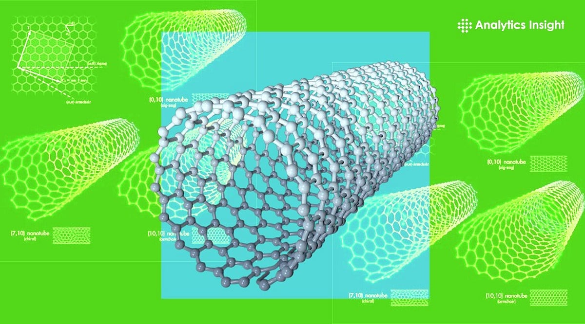
    A carbon nanotube is formed when a thin sheet of carbon atoms rolls into a hollow tube. Some nanotubes consist of a single layer, while others have multiple concentric layers. They are just a few nanometers wide but can grow to several centimeters in length. These structures are incredibly lightweight yet about 100 times stronger than steel on a weight-for-weight basis. They also conduct electricity exceptionally well—some behave like metals, others like semiconductors—and efficiently transfer heat, helping electronic devices stay cool during operation.

    Revolutionizing AI Chip Performance

    Artificial intelligence demands powerful computer chips, and traditional silicon is nearing its physical limits. Smaller silicon chips generate more heat and consume more electricity. Carbon nanotubes offer a solution through transistors that move electricity with minimal resistance, enabling AI chips to operate faster and more efficiently. Their superior heat dissipation also helps chips run cooler, extending lifespan and reducing energy consumption in large data centers. While commercial adoption is still in development, carbon nanotubes are emerging as a leading candidate for next-generation computing.

    Advancing Electric Vehicle Batteries

    In EV batteries, carbon nanotubes don’t replace lithium but significantly improve battery performance. They facilitate better electrical flow, leading to faster charging, increased capacity, and longer cycle life. Because only tiny amounts are needed, more space remains for energy storage, potentially allowing larger batteries without added weight. Carbon nanotubes also stabilize silicon anodes, which can store more energy than traditional graphite anodes, further boosting battery efficiency and durability.

    Transformative Healthcare Applications

    Medicine stands to benefit greatly from carbon nanotubes. They can serve as targeted drug delivery vehicles, carrying medicine directly to diseased cells while sparing healthy tissue and reducing side effects. In cancer treatment, nanotubes absorb near-infrared light and convert it to heat, which can destroy tumors with minimal collateral damage. Additionally, carbon nanotube-based sensors are highly sensitive, enabling early disease detection through tiny changes in the body. Flexible health monitors made from these materials could track heart rate, blood sugar, and other vital signs continuously.

    Remaining Challenges

    Despite their promise, several hurdles must be overcome. High-quality carbon nanotubes remain expensive to produce, and manufacturing methods need to scale while ensuring uniformity. Long-term safety studies are essential before medical applications become routine, and industry-wide quality standards are still being developed.

    The Road Ahead

    Carbon nanotubes are already used in some batteries, electronics, and composite materials. As production improves, their adoption will accelerate. Experts project the global carbon nanotube market will grow from approximately $8.8 billion in 2026 to nearly $24.5 billion by 2034, driven by AI, EVs, healthcare, electronics, and energy storage. Though tiny, carbon nanotubes hold immense potential to power faster AI, smarter medical devices, and more efficient energy systems.

    Frequently Asked Questions

    1. What are carbon nanotubes?

    Carbon nanotubes are minuscule hollow tubes made of carbon atoms. They are extraordinarily strong, lightweight, and excellent conductors of electricity and heat.

    2. Why are carbon nanotubes important for AI chips?

    They enable transistors that switch faster and generate less heat, leading to AI chips that are more powerful and energy-efficient than current silicon-based designs.

    3. How do carbon nanotubes improve EV batteries?

    They enhance electrical conductivity inside the battery, supporting faster charging, higher energy density, and longer lifespan, and also help stabilize advanced anode materials.

    4. Can carbon nanotubes be used in healthcare?

    Yes, research is exploring them for targeted drug delivery, thermal cancer ablation, ultra-sensitive disease detection, and wearable health monitors.

    5. What are the main challenges?

    High production costs, scalability issues, quality control, and rigorous safety testing are the primary barriers to widespread adoption.

  • Exploring the Frontiers of 2D Materials: MIT’s Latest Breakthroughs in Superconductivity, Transistors, and Quantum Computing

    Exploring the Frontiers of 2D Materials: MIT’s Latest Breakthroughs in Superconductivity, Transistors, and Quantum Computing

    MIT researchers continue to push the boundaries of two-dimensional (2D) materials, unveiling a series of groundbreaking discoveries that promise to revolutionize electronics, quantum computing, and material science. From terahertz microscopes revealing superconducting electron motion to atom-thin transistors grown directly on silicon chips, these advances highlight the immense potential of 2D materials.

    Terahertz Microscope Reveals Superconducting Electron Motion

    For the first time, physicists used a novel terahertz microscope to observe the ‘jiggling’ of superconducting electrons in a fluid state. This breakthrough, reported on February 4, 2026, offers unprecedented insights into the dynamics of superconductivity.

    FabObscura: Turning Everyday Objects into Animated Displays

    On September 10, 2025, MIT introduced FabObscura, a software tool that enables users to design and print barrier-grid animations without electronics. This system transforms household items into dynamic, eye-catching displays, blending creativity with technology.

    Unexpected Magnetism in Atomically Thin Materials

    Physicists discovered and explained unexpected magnetism in an atomically thin material on January 23, 2025. This finding opens a new platform for studying quantum materials and their exotic properties.

    High-Rise 3D Chips: Stacking Transistors for AI Hardware

    On December 18, 2024, MIT engineers unveiled a technique to grow ‘high-rise’ 3D chips, exponentially increasing transistor density. This innovation could lead to more efficient AI hardware by stacking electronic components vertically.

    Non-Abelian Anyons: Exotic Matter for Quantum Computing

    MIT physicists predicted the formation of non-Abelian anyons without a magnetic field on November 18, 2024. These fractionalized electrons could enable robust quantum computing and open new avenues for basic research.

    Superlative Transistor Properties for Broad Electronics

    On July 26, 2024, researchers demonstrated a new transistor made from an ultrathin material that meets or exceeds industry standards. It offers superfast switching and extreme durability, promising broad applications in electronics.

    Superconductivity from Quasicrystals

    On October 11, 2023, physicists coaxed superconductivity from quasicrystals, creating a flexible platform for studying exotic phenomena and potentially leading to new materials.

    Powerful Tool for Tuning Atomically Thin Materials

    An international team reported a powerful tool for studying and tuning atomically thin materials on June 27, 2023. This work could lead to novel electronic applications.

    Atomically Thin Transistors Grown on Computer Chips

    On April 27, 2023, MIT engineers developed a low-temperature growth technique to integrate 2D materials directly onto silicon circuits, enabling denser and more powerful chips.

    Skyrmions: Recipe for Exotic Phenomena

    Physicists predicted new phenomena involving skyrmions on March 17, 2023, offering a recipe for realizing them. These could have applications in future computers and beyond.

    Superconductivity Switching in Magic-Angle Graphene

    On January 30, 2023, a study showed that a quick electric pulse can flip the electronic properties of magic-angle graphene, enabling ultrafast, brain-inspired superconducting electronics.

    Perfect Atom-Thin Materials on Industrial Silicon Wafers

    MIT engineers grew ‘perfect’ atom-thin materials on industrial silicon wafers on January 18, 2023, allowing chip manufacturers to produce next-generation transistors beyond silicon.

    Dresselhaus Lecture on Moiré Quantum Matter

    On December 21, 2022, Professor Pablo Jarillo-Herrero delivered the Dresselhaus Lecture, discussing moiré quantum matter and its potential for investigating strongly correlated and topological physics.

    Expanding 2D Materials: New Measurement Technique

    A new technique reported on November 18, 2022, accurately measures how atom-thin materials expand when heated, aiding the development of faster, more powerful electronic devices.

    Family of Robust Superconducting Graphene Structures

    On July 8, 2022, physicists discovered a family of robust superconducting graphene structures, which could inform the design of practical superconducting devices.