Category: AI Chips

  • Why Chip Packages Are the Front Line of AI Hardware’s Thermal Challenge

    Why Chip Packages Are the Front Line of AI Hardware’s Thermal Challenge

    Most discussions about AI hardware focus on the chips themselves: more compute, faster interconnects, and larger models packed onto denser infrastructure. But every one of those gains carries a physical consequence that software alone cannot fix. More compute means more heat, and that heat must escape through an increasingly constrained space.

    AI’s Growing Power Problem Starts Inside the Package

    The International Energy Agency estimates that data centers consumed roughly 415 TWh of electricity in 2024 and could approach 945 TWh by 2030, with AI infrastructure driving much of that growth. Yet the true origin of the thermal challenge is often overlooked. It does not begin at the rack or even at the cold plate. It begins right at the chip package, where dense compute creates intense localized heat.

    As AI accelerators and high-performance processors shrink their footprints, the heat they produce is concentrated into tighter areas. Fans, cold plates, and liquid loops can move heat away from the system, but none of that cooling matters if the heat cannot first leave the chip package cleanly.

    The Critical First Handoff: Small Parts, Big Thermal Impact

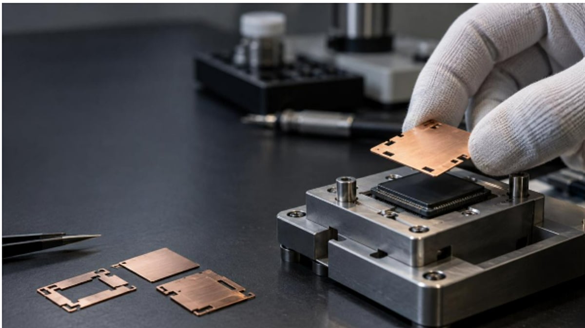
    The first stage of the thermal path is easy to miss because it is physically small. Heat spreaders, thin copper or aluminum layers, shims, package lids, shielding pieces, and other precision metal parts bridge the concentrated heat source to the next cooling stage. These are not the large server heat sinks most people picture. They are thin, drawing-defined components sitting closest to the chip, where cramped space, tight interfaces, and high local heat density turn tiny manufacturing details into major performance factors.

    Intel describes the integrated heat spreader as the part attached to the processor package that provides a mating surface for the thermal solution above it. That handoff is decisive. A thermal part may be nothing more than a thin piece of metal, yet it determines how efficiently heat reaches the next layer of the stack. If it does not fit flat or hold a controlled interface, the entire cooling system above it can be capped before heat ever reaches the cold plate.

    Material choice alone does not guarantee performance. Copper offers excellent thermal conductivity, while aluminum provides lower weight and easier fabrication, but neither metal ensures good thermal transfer by itself. Geometry, flatness, surface condition, and assembly quality determine what the material actually delivers.

    Flatness and Precision Are Thermal Performance

    Thermal performance depends on a controlled interface between the spreader, the thermal interface material, and the cooling layer that follows. Flatness and coplanarity keep gaps small, and small gaps keep thermal resistance low. Thermal interface materials can fill minor surface irregularities, but they cannot rescue poor geometry or an oversized gap. Intel’s own guidance notes that the gap between a spreader and a heat-sink base directly drives thermal resistance, and that the flatness of both surfaces sets that gap.

    For compact AI hardware, this translates into a demanding set of simultaneous requirements:

    • The metal must stay flat through fabrication and assembly, resisting warpage even when thin.
    • Its profile must respect keep-out areas around chips, modules, and boards.
    • Edges must be clean enough to avoid fouling mating surfaces or neighboring components.
    • Fine openings, tabs, locating features, or vent structures may be required.
    • The part must repeat dimension for dimension from prototype through qualification into production.

    A component that looks trivial on a drawing becomes difficult once it has to be thin, flat, feature-dense, and identical part after part.

    Manufacturing for Function, Not Arbitrary Tolerances

    Small deviations may be acceptable on ordinary parts as long as the piece fits. In a thermal assembly, the same deviation can change interface pressure, gap thickness, contact consistency, or the position of adjacent parts. The stakes on a dimension are simply higher when heat has to cross it.

    That does not mean over-specifying every feature. Tightening all dimensions drives up cost and slows production without real benefit. The key is identifying which dimensions affect thermal contact, assembly alignment, and finished-device performance, then controlling those tightly while treating less critical features practically. On a small chip-level thermal part, flatness, profile accuracy, edge condition, and a clean finished surface usually matter more than chasing the tightest possible number on every dimension.

    Matching the Manufacturing Process to the Part

    Large, stable, high-volume heat sinks are often best produced by extrusion, casting, or conventional machining, and those methods remain efficient for standard cooling jobs. But they are not always suitable for thin, custom, feature-dense parts living close to a chip. When a thermal component has a changing layout, fine features, thin material, or a design still moving through prototype revisions, the manufacturing route must fit both the geometry and the production stage.

    This is where precision thermal parts earn their place: thin heat spreaders, thermal shims, fine-featured covers, and custom metal layers built around a specific package rather than a generic heat-sink profile. Making precision heat sink parts with controlled interfaces, thin and flat, is a different task from cutting a finned block. It requires a process chosen to produce the part reliably, inspect it meaningfully, and hold up at the required volume. No single process replaces all others; the part simply has to be matched to the method that can actually make it.

    Design for Manufacture Is Essential in AI Hardware

    The strongest thermal designs bring manufacturing considerations in early. Before a drawing is frozen, the team should know which surfaces must stay flat, which features affect assembly, how thin the material can be, and how the finished part will be inspected. This matters more in AI hardware than almost anywhere else because design cycles are fast and package layouts keep shifting. A part that works for one prototype but cannot be produced the same way at volume is a production risk waiting to surface.

    Getting thermal engineers, package designers, and manufacturers into the same conversation early prevents that risk. It helps the team identify which requirements are truly critical, which can be relaxed, and which process fits the part in hand.

    AI’s Thermal Constraint Is a Manufacturing Constraint

    AI hardware will continue to put more pressure on every part of the thermal path. Data-center infrastructure, liquid cooling, and system-level design all matter, but the path still begins at the chip package, where heat must first cross a small, carefully controlled interface. The parts closest to that interface are thin, quiet, and easy to miss. They are also becoming harder to make and more important to get right.

    As AI chips run hotter and cooling space continues to tighten, the precision metal parts that spread, bridge, shield, and steer heat become a genuine factor in hardware performance. The wall in front of AI is a cooling problem, and underneath it, a manufacturing problem.


  • Snapdragon Summit 2026: Qualcomm’s Flagship Chip Reveals Set for September 22

    Snapdragon Summit 2026: Qualcomm’s Flagship Chip Reveals Set for September 22

    Qualcomm’s Snapdragon Summit 2026 kicks off on September 22 in Maui, Hawaii, running through September 24. The opening day will focus heavily on mobile platforms and the company’s vision for the ‘agentic AI’ era.

    Two New Snapdragon 8 Elite Chips Expected

    The highlight is anticipated to be Qualcomm’s next flagship smartphone processors. Leaks indicate the Snapdragon 8 Elite Gen 6 and Snapdragon 8 Elite Gen 6 Pro, both likely built on a 2nm manufacturing process for notable gains in performance and power efficiency. The Pro variant may support faster LPDDR6 memory and UFS 5.0 storage, while the standard model could retain LPDDR5X. Upgraded graphics, including Adreno Matrix Cores and Adreno Neural Fusion for AI workloads, are also confirmed by Qualcomm.

    AI, XR and PCs Take Center Stage

    Beyond phones, the summit will emphasize agentic AI across personal computing, sound, and extended reality. Qualcomm’s Snapdragon portfolio now includes PCs, XR devices, wearables, and automotive platforms, positioning the summit as a key venue for its cross-device AI push.

    Xiaomi, iQOO and OnePlus Linked to Early Adoption

    The new chips are expected to reach smartphones swiftly. Xiaomi, iQOO, and OnePlus are among brands rumored to launch devices with the next-generation platforms, with the first wave possibly arriving in India by late 2026 or early 2027. Official specifications, performance claims, and partner announcements will be unveiled at the summit.

  • India’s Semicon 2.0 Program Targets 200 New Chip Design Firms

    India expects around 200 chip design companies to emerge under its Semicon 2.0 programme as the government expands support for semiconductor design, manufacturing and research. Union Electronics and Information Technology Minister Ashwini Vaishnaw said the new companies could strengthen India’s domestic chip design base. The government is building on the first phase of the India Semiconductor Mission, which supports startups with design tools, funding and technical resources.

    Semicon 2.0 Targets Growth in India’s Chip Design Sector

    Vaishnaw said India’s existing strength in information technology and global capability centres is now extending into semiconductor design. “We estimate at least 200 chip design companies emerging under Semicon 2.0,” he said during a fireside chat.

    Under the first phase of the India Semiconductor Mission, the government focused on reducing the high cost of Electronic Design Automation tools. More than 105 chip design startups received access to advanced EDA tools, which companies use to develop, test and verify semiconductor designs.

    The government said 20 of these startups also secured venture capital funding. The funding has helped some firms move beyond early product development and work towards commercial applications. Semiconductor startups are also developing chips for use in different products.

    India has also expanded training for semiconductor professionals. Around 70,000 chip-design engineers have received training over the past four years, against a target of 85,000. The government expects this workforce to support chip design, research, manufacturing and related activities.

    Semiconductor Plants Begin Commercial Production

    India is also increasing domestic semiconductor manufacturing capacity. According to Vaishnaw, five of the 12 semiconductor plants approved under the first phase of the India Semiconductor Mission have started commercial production.

    The government is now focusing on applied research and development inside manufacturing plants. Vaishnaw said this work should improve product quality and manufacturing processes. The electronics manufacturing sector has also helped Indian micro, small and medium enterprises build precision manufacturing skills used across electronics, aerospace, defence and semiconductor production.

    The government is also working with companies on local production of critical semiconductor equipment and materials. Vaishnaw said Indian companies and overseas partners have started discussions and signed agreements related to machinery and key materials.

    He added that semiconductor production facilities will use water recycling systems to reduce fresh water use. The government is also encouraging data centres and manufacturing facilities to use closed-loop cooling systems where possible.

    Global Partners Explore Semiconductor Opportunities in India

    SEMICON India 2026 brought companies and government representatives from several major semiconductor markets together to discuss investment and supply-chain cooperation. Participants included companies from the United States, Japan, Singapore, South Korea, the Netherlands and Finland.

    “The country roundtables are basically showing that companies from those countries can expand their work here,” Vaishnaw said. He added that overseas governments were supporting companies that were exploring opportunities in India.

    The India-Singapore Country Roundtable attracted 142 participants and discussed manufacturing, advanced packaging and supply-chain management. The India-Europe session had 139 participants and covered investment, equipment, materials, manufacturing, chip design, research and talent development.

    Meanwhile, the India-South Korea Country Roundtable brought together 115 participants. Discussions covered semiconductor manufacturing, materials, advanced packaging, technology, investment and supply chains.

    Foreign Secretary Vikram Misri said resilient semiconductor supply chains require trusted international partnerships. He identified reliability, credibility, incentives and value creation as key areas for cooperation while calling for a balance between domestic capabilities and international partnerships.

    India’s Semicon 2.0 programme will now focus on expanding chip design, manufacturing, research, equipment production and skilled talent while bringing more domestic and international companies into the semiconductor ecosystem.

  • Beyond GPUs: Emerging Technologies Reshaping the AI Infrastructure Race

    Beyond GPUs: Emerging Technologies Reshaping the AI Infrastructure Race

    The era of GPU-only AI infrastructure is being challenged by a growing wave of specialized hardware and computing paradigms. As large-scale AI models continue to demand more performance and efficiency, companies are exploring alternatives that promise faster training, lower power consumption, and greater flexibility. Here is a closer look at the key technologies entering the AI infrastructure race.

    Google TPU

    Google’s Tensor Processing Units are built specifically for AI workloads, with specialized matrix processing that provides a strong alternative to general-purpose GPU acceleration for large-scale models.

    AWS Trainium

    Amazon’s Trainium accelerators are designed to handle machine-learning training workloads, helping cloud customers reduce their dependence on GPUs while optimizing both performance and infrastructure costs.

    Cerebras Wafer-Scale Engine

    Cerebras has developed enormous wafer-scale processors containing thousands of processing cores. This specialized architecture is built to address demanding AI model training workloads.

    Groq LPU

    Groq’s Language Processing Units focus on fast inference, using a specialized hardware architecture to deliver predictable performance for large language model workloads.

    Photonic Computing

    Photonic processors use light to perform computations, potentially delivering high bandwidth and energy efficiency for increasingly demanding artificial intelligence workloads.

    Processing-In-Memory

    Processing-in-memory architectures bring computation closer to stored data, reducing memory movement and potentially improving efficiency across large-scale AI workloads.

    Neuromorphic Chips

    Neuromorphic processors mimic aspects of biological neural systems, targeting highly efficient AI computation through event-driven processing and specialized hardware architectures.

    Quantum Computing

    Quantum processors could eventually address specialized optimization and scientific workloads, offering a fundamentally different computing paradigm beyond conventional GPU-based AI infrastructure.

    ASIC Accelerators

    Application-specific integrated circuits are designed for particular AI workloads, enabling companies to optimize performance, power consumption, and infrastructure for targeted applications.

    As the demand for advanced AI continues to grow, the infrastructure race is no longer limited to GPUs. These emerging technologies are shaping a more diversified ecosystem of compute options, each with unique strengths for the next stage of AI development.

  • Apple’s M8 Ultra AI Server Plans Signal a Comeback Years After Xserve

    Apple’s M8 Ultra AI Server Plans Signal a Comeback Years After Xserve

    Apple is reportedly preparing to re-enter the server market with a new line of AI-focused systems built around its upcoming M8 Ultra chips. The move would mark the company’s return to enterprise hardware nearly 15 years after it discontinued the Xserve line.

    According to people familiar with the plans, Apple is developing AI servers in two configurations: one powered by two M8 Ultra chips and a larger variant with four. The company is also said to be evaluating NVIDIA’s NVLink Fusion interconnect technology to link the processors. A launch could happen around 2029, though the project is still in flux and Apple may alter or abandon it.

    The reported effort comes as AI companies increasingly turn to Mac mini and Mac Studio systems for local AI workloads. Apple already operates servers for Private Cloud Compute, which handles some Apple Intelligence tasks off-device, and it has been working with Google and NVIDIA to expand that infrastructure. A dedicated server line would give Apple another channel to deploy its own silicon in enterprise AI environments.

    Can Apple Succeed Where Xserve Failed?

    Selling servers to large organizations is a different challenge from selling iPhones and Macs. Enterprise buyers expect long-term support, robust systems management, strong security, and compatibility with existing business software—areas where Apple has limited experience in the data center since ending Xserve in 2011.

    The reported M8 Ultra server plan highlights how quickly AI is reshaping Apple’s hardware roadmap. The bigger test is whether Apple can translate its consumer-chip strengths into a credible enterprise server business.

  • MediaTek Dimensity 9600 Pro: The Next Leap in AI-Powered Flagship Chips

    MediaTek Dimensity 9600 Pro: The Next Leap in AI-Powered Flagship Chips

    MediaTek has unveiled its latest flagship processor, the Dimensity 9600 Pro, positioning it as a transformative step for next-generation smartphones. Built on TSMC’s 2nm process, this chip integrates a fourth-generation all-big-core CPU, a dual-NPU architecture, LPDDR6 memory support, and UFS 5.0 storage. MediaTek claims significant gains in performance, power efficiency, and on-device AI capabilities, setting a new standard for premium mobile hardware.

    Key Takeaways

    • The Dimensity 9600 Pro uses a 2nm process with an all-big-core CPU, claiming major performance and efficiency improvements.
    • Its dual-NPU design supports advanced on-device AI, handling models up to 30 billion parameters.
    • LPDDR6, UFS 5.0, stronger graphics, and advanced camera features mark a comprehensive hardware upgrade for flagships.

    A Revolutionary 2nm Design

    The Dimensity 9600 Pro is MediaTek’s first mobile chip built on a 2nm process. Its CPU configuration includes two Arm C2-Ultra cores at up to 4.55GHz, three Arm C2-Pro cores at 4.35GHz, and three additional Arm C2-Pro cores at 3.1GHz. This fourth-generation all-big-core architecture also incorporates a 21% larger L2 cache.

    MediaTek’s internal benchmarks show a 17% increase in single-core performance with 37% better power efficiency, while multi-core tasks see a 15% performance boost and a remarkable 61% reduction in power consumption. These figures, however, come from lab tests and may vary in real-world devices depending on thermal design, battery size, and software optimization.

    AI Takes Center Stage

    The chip features two neural processing units (NPUs): the NPU 1090 for heavy on-device AI tasks and the Super Efficient NPU 2.0 for low-power, always-on AI operations. MediaTek claims a 51% improvement in large language model (LLM) prefill performance and a 55% gain in token generation per watt. The platform supports on-device models with up to 30 billion parameters, aided by a compression engine that reduces memory footprint and support for Mixture of Experts (MoE) architecture.

    The Super Efficient NPU 2.0 also cuts power consumption for always-on AI by 40%, a critical factor for AI assistants that continuously access phone data, sensors, and apps.

    Memory and Storage Advancements

    With first-wave support for LPDDR6 memory and UFS 5.0 storage, the Dimensity 9600 Pro delivers substantial improvements in data throughput. UFS 5.0 offers twice the read and write speeds of its predecessor, while LPDDR6 increases effective memory bandwidth by 33% at the same frequency. A larger 34.5MB cache further enhances overall system responsiveness.

    Graphics Performance for High Frame Rates

    The new G2-Ultra NX GPU delivers up to 27% higher peak performance, 24% lower power consumption at peak, and up to 18% faster ray-tracing. The chip can support native gameplay above 185fps. MediaTek integrates the GPU with the NPU through its Neural Graphics Architecture, enabling AI-assisted graphics rendering and super-resolution tasks.

    Camera and Imaging Upgrades

    The Imagiq 1290 image signal processor (ISP) pairs with an AI Imaging Fusion Architecture to support 60fps subject focus, 4K240 slow-motion video, 4K60 AI True Color Tone, and 4K120 cinematic log. The system also handles 17EV dynamic range imaging, 4K live photo with full depth of field, H.266 hardware video decode, and MV-HEVC for spatial video—all without relying on cloud services.

    First Phones and Real-World Testing

    MediaTek has announced that the first Dimensity 9600 Pro phones will arrive this quarter. According to Reuters, Xiaomi, OPPO, and vivo are among the manufacturers collaborating with MediaTek. OPPO has confirmed the Find X10 Pro Max with this chip, slated for a September 22 launch in China.

    The true test lies in how these devices perform in the real world. MediaTek’s claims are based on its own lab tests, so independent reviews will be crucial to verify whether retail units match the stated figures.

    What the 9600 Pro Changes

    The Dimensity 9600 Pro shifts the focus from raw CPU speed to a balanced integration of CPU, GPU, NPU, memory, storage, and camera hardware. Its 2nm foundation and dual-NPU design amplify the role of on-device AI, while faster memory and storage enable a smoother user experience. For the next wave of premium smartphones, this chip signals a clear direction: high-performance processing, advanced graphics, powerful local AI, and cutting-edge camera capabilities must work as a cohesive system.

    Frequently Asked Questions

    1. What is the Dimensity 9600 Pro?

    The Dimensity 9600 Pro is MediaTek’s flagship smartphone processor featuring a 2nm design, advanced CPU and GPU hardware, dual-NPU AI, and support for LPDDR6 and UFS 5.0.

    2. How powerful is the Dimensity 9600 Pro?

    MediaTek claims up to 17% higher single-core performance, 15% higher multi-core performance, and a 61% reduction in multi-core power usage compared to its stated previous-generation baseline.

    3. What AI features does the chip offer?

    The dual-NPU system supports on-device AI models with up to 30 billion parameters, along with improved AI performance per watt and a dedicated super-efficient NPU for always-on tasks.

    4. Does the Dimensity 9600 Pro support advanced gaming?

    Yes. Its G2-Ultra NX GPU provides higher peak graphics performance, faster ray tracing, and support for native gameplay above 185fps.

    5. What memory and storage does the Dimensity 9600 Pro support?

    The platform supports LPDDR6 memory and UFS 5.0 storage, along with a generous 34.5MB cache for improved data throughput.

  • A20 Pro vs Earlier Apple Chips: 7 Major Upgrades to Expect in iPhone Performance

    A20 Pro vs Earlier Apple Chips: 7 Major Upgrades to Expect in iPhone Performance

    Apple’s next-generation A20 Pro chip is shaping up to be one of the most significant leaps forward in iPhone performance in recent years. With a new manufacturing process and refinements across the board, the A20 Pro could offer major improvements over the A17 Pro, A18 Pro, and A19 Pro. Here are seven key upgrades that may help it stand apart from previous Apple silicon.

    1. Built on TSMC’s 2nm Process

    The A20 Pro is expected to be Apple’s first iPhone chip manufactured on TSMC’s 2nm process. Moving to a smaller process node allows more transistors to fit into the same physical space, which can boost both performance and power efficiency.

    2. Faster Overall Performance

    Thanks to the 2nm transition, the A20 Pro could deliver a meaningful performance jump over earlier A-series chips. Users may notice smoother multitasking, faster app launches, and improved responsiveness in demanding tasks like gaming, video editing, and AI-heavy workloads.

    3. Better Power Efficiency

    Performance gains are only part of the story. The newer manufacturing technology is also expected to improve energy efficiency, allowing the A20 Pro to handle more intensive tasks while consuming less power. That could translate into better battery life during heavy use.

    4. Smarter On-Device AI Processing

    Apple has been expanding AI features across the iPhone, and the A20 Pro is expected to push that further. Improvements to on-device AI processing could enable future iPhones to run more sophisticated intelligent features locally, reducing the need to rely heavily on cloud computing.

    5. Stronger Graphics Performance

    The A20 Pro is also rumored to bring a significant boost to graphics. A more capable GPU would benefit high-end mobile games, advanced camera effects, video editing, and other graphics-intensive applications that push the iPhone’s hardware to its limits.

    6. Better Thermal Management

    As chips become more powerful, managing heat becomes increasingly important. The A20 Pro’s new architecture and manufacturing process could help Apple balance sustained performance with heat and power consumption, so the device stays cool even during extended demanding sessions.

    7. More Efficient Memory Design

    The A20 Pro is expected to refine how the chip interacts with memory. Improved memory efficiency could help demanding apps run more smoothly, especially when switching between multiple apps or performing intensive creative and AI workloads.

    A New Benchmark for Apple Silicon

    From the A17 Pro and A18 Pro to the A19 Pro, Apple has steadily advanced its in-house chip designs. The A20 Pro could continue that trend with a substantial upgrade in both efficiency and raw power, potentially setting a new standard for future iPhones.

  • Intel and SK Hynix Shares Surge Following Reports of AI Chip Partnership Talks in Ohio

    Intel and SK Hynix Shares Surge Following Reports of AI Chip Partnership Talks in Ohio

    Reports that Intel and SK hynix are in discussions for a potential partnership to manufacture memory chips at Intel’s Ohio campus have sent shares of both companies higher. Intel shares rose approximately 4%, while SK hynix gained around 3% on Wednesday, September 16.

    The potential deal would see SK hynix produce chips at Intel’s $100 billion Ohio site, though no agreement has been signed yet. The talks come at a time when AI companies are increasingly demanding high-bandwidth memory chips for servers and data centers. SK hynix is a leading supplier of such memory, widely used in AI systems.

    Intel has faced delays at its Ohio project, originally expected to begin production in 2025. A partnership with SK hynix could provide a new purpose for the site while expanding memory chip production in the United States.

    SK hynix already has a chip packaging plant under construction in Indiana, but it does not yet manufacture memory chips in the U.S. Moving some production to Ohio would help the company establish a larger footprint in the country.

    Ohio’s Role in the AI Chip Race

    The possible collaboration could benefit both companies. Intel could repurpose its delayed Ohio facility, while SK hynix would gain another location for memory production closer to U.S. customers.

    The timing is crucial as the AI race intensifies, with companies demanding powerful chips for advanced AI systems. Increasing local production could help meet this demand over time.

    However, the talks remain at an early stage, and any deal could face cost and technology hurdles. South Korea may also review an agreement involving advanced memory technology. If the plan moves forward, Intel’s Ohio site could play a new role in the growing U.S. AI chip supply chain.

  • Anthropic CEO Urges Slower AI Development, Sparking Pressure on Chip Stocks

    Anthropic CEO Urges Slower AI Development, Sparking Pressure on Chip Stocks

    Anthropic CEO Dario Amodei’s recent call to slow the pace of advanced AI development is creating near-term headwinds for semiconductor and technology stocks. However, sustained demand for chips, data centers, and computing infrastructure may limit the long-term market impact.

    Anthropic Advocates for Measured AI Progress

    In a September essay, Amodei urged AI companies to prioritize safety by adopting a more deliberate development pace. He emphasized that this is not a halt to training models but a call for stronger safety checks and independent third-party evaluations. OpenAI CEO Sam Altman supported the initiative, and xAI owner Elon Musk publicly agreed with Amodei’s stance. Anthropic has also committed to granting independent evaluators ongoing access to review its safety practices.

    Market Reaction and Chip Stock Vulnerability

    The warnings could amplify selling pressure on semiconductor stocks, which have already experienced weakness. The Nasdaq 100 has fallen over 4% from its June peak, and a U.S. chip-stock gauge dropped roughly 14%. Asian technology shares have declined nearly 8% in the same period. Portfolio manager Gary Tan of Allspring Global Investments noted that while short-term pressure is likely, the longer AI investment cycle remains intact. The market’s focus will be on whether slower model development alters future chip orders.

    AI Infrastructure Spending Remains Robust

    Despite the slowdown rhetoric, spending on AI infrastructure continues to underpin chipmakers and suppliers. Investments in processors, memory, networking equipment, cooling systems, data centers, and power capacity remain strong. Many projects are already underway, limiting the immediate effect of a slower model cycle on spending plans. Investment strategist Billy Leung of Global X Management pointed out that a longer development timeline could allow companies to generate more revenue from existing systems, shifting emphasis toward commercialization and broader AI adoption.

    Broader Market Conditions Add Pressure

    Technology stocks also face headwinds from rising interest rate expectations, which can weigh on high-growth, high-valuation names. As a result, semiconductor and AI shares remain sensitive to any changes in spending, earnings, or model development plans. Still, demand for computing power persists. Charu Chanana, chief investment strategist at Saxo Markets, suggested that added safeguards could spur further investment in cybersecurity and AI monitoring tools. Early market signals, such as SK Hynix-linked perpetual futures on Hyperliquid falling about 2.5% as of Sunday afternoon in Singapore, indicate caution before traditional markets reopen.

  • AI Demand Drives These Semiconductor Stocks: NVIDIA, TSMC, and More

    AI Demand Drives These Semiconductor Stocks: NVIDIA, TSMC, and More

    Artificial intelligence continues to reshape the semiconductor landscape, creating opportunities for investors across the chip supply chain. From GPU leaders to memory manufacturers and equipment providers, several stocks are positioned to benefit from surging AI demand. Below, we analyze the key players and the risks that accompany their growth.

    Key Takeaways

    • NVIDIA remains the dominant AI chip supplier, while Broadcom provides exposure to custom silicon and networking.
    • TSMC and Micron gain from advanced manufacturing and high-bandwidth memory demand.
    • Equipment firms like ASML, Lam Research, Applied Materials, and KLA offer indirect AI growth avenues.

    NVIDIA and Broadcom Lead the AI Chip Race

    NVIDIA’s position as the premier AI chipmaker is unshaken. With its stock near $218.36 and a market capitalization approaching $5.30 trillion, the company supplies GPUs and networking solutions for AI data centers. A 2.26% dip on September 10 reflected broader tech pressure from rising Treasury yields, but its long-term trajectory remains tied to AI deployment.

    Broadcom offers a complementary play. Trading around $360.83, it designs custom AI chips and networking hardware for large tech firms. This diversification allows investors to tap AI growth beyond the GPU market.

    AMD adds a third option. At roughly $521.10, it has gained over 143% year-to-date, competing with NVIDIA through its AI accelerators and EPYC server processors. However, such sharp gains introduce higher valuation risk.

    TSMC and Micron: Supply Chain Pillars

    TSMC is the linchpin of advanced chip fabrication. Its U.S.-listed shares trade near $435.36, valuing the company at $1.58 trillion. The foundry posted record August revenue of NT$514.806 billion, up 53.3% year-over-year, with July revenue also strong at NT$467.580 billion. TSMC forecasts Q3 revenue between $44.6 billion and $45.8 billion, and plans capital expenditure of $60–$64 billion in 2026.

    Micron focuses on high-bandwidth memory (HBM), essential for AI workloads. With shares around $1,028, the company aims to boost HBM output to 100,000 wafers per month by year-end. HBM shortages are raising chip costs, but new entrants and rapidly shifting memory markets add risk. Micron’s fiscal Q4 results on September 30 will be a key catalyst.

    Equipment Stocks Provide Alternative Exposure

    Lam Research, Applied Materials, and KLA supply tools for chip manufacturing. Lam Research trades near $301.06, Applied Materials at $469, and KLA at $177.18—each fell over 3% on September 10. Their fortunes rise with fab expansions, not AI chips directly, making them a different risk-reward proposition.

    Marvell sits at the intersection of custom silicon and connectivity, with a stock price of $235.01 and a 176.55% year-to-date gain. Its high valuation amplifies downside risk.

    ASML stands out as the sole supplier of EUV lithography systems, crucial for shrinking process nodes. Closing near $1,698 on September 10, ASML’s technology monopoly gives it a long-term edge, though its stock can swing with capital spending cycles.

    The AI Chip Trade Faces New Tests

    Strong AI demand does not immunity from broader market forces. Higher oil prices and rising Treasury yields pressured tech stocks, and the broader U.S. market fell on September 10. Yet TSMC’s sales and HBM demand underscore robust chip demand, providing a solid business foundation amid stock volatility.

    NVIDIA, Broadcom, and TSMC offer the widest AI exposure. Micron and AMD provide targeted plays on memory and GPU alternatives. Lam Research, Applied Materials, KLA, and ASML serve the equipment segment. Marvell carries higher potential but also higher risk.

    Investors should monitor chip sales, HBM supply, AI data center budgets, and capital expenditure plans. The critical question is whether supply, capacity, and profits can keep up with the lofty expectations already baked into these stocks.

    FAQs

    Which semiconductor stock has the strongest AI exposure?

    NVIDIA has the most direct AI exposure through its GPUs and data center products.

    Why is TSMC important to AI growth?

    TSMC manufactures advanced chips for major tech firms, forming the backbone of AI processor supply.

    Why has Micron gained attention?

    Micron is a key supplier of high-bandwidth memory, critical for AI data center performance.

    Which semiconductor stocks offer equipment exposure?

    ASML, Lam Research, Applied Materials, and KLA provide exposure to chip manufacturing equipment.

    Are semiconductor stocks low-risk investments?

    No. Even with strong chip demand, share prices can decline due to high valuations, market conditions, and changing expectations.

    Disclaimer: This article is for informational purposes only and does not constitute financial advice. Investing in stocks involves risk, including potential loss of principal. Always conduct your own research before making investment decisions.